OSP Finish on PCB: Pros and Cons
Author : Adrian October 07,solder paste injection 2025Table of Contents
If you're looking for a cost-effective and environmentally friendly surface finish for your printed circuit board (PCB), OSP (Organic Solderability Preservative) might be the solution. But what exactly is OSP, and what are its advantages and limitations? In short, OSP is a thin organic coating that protects copper pads from oxidation while ensuring good solderability during assembly. Its pros include low cost, eco-friendliness, and ease of rework, while its cons involve limited shelf life and sensitivity to handling. In this detailed blog, we'll dive deeper into the OSP finish on PCB, exploring its pros and cons to help you decide if it's the right choice for your project.
What is OSP Finish on PCB?
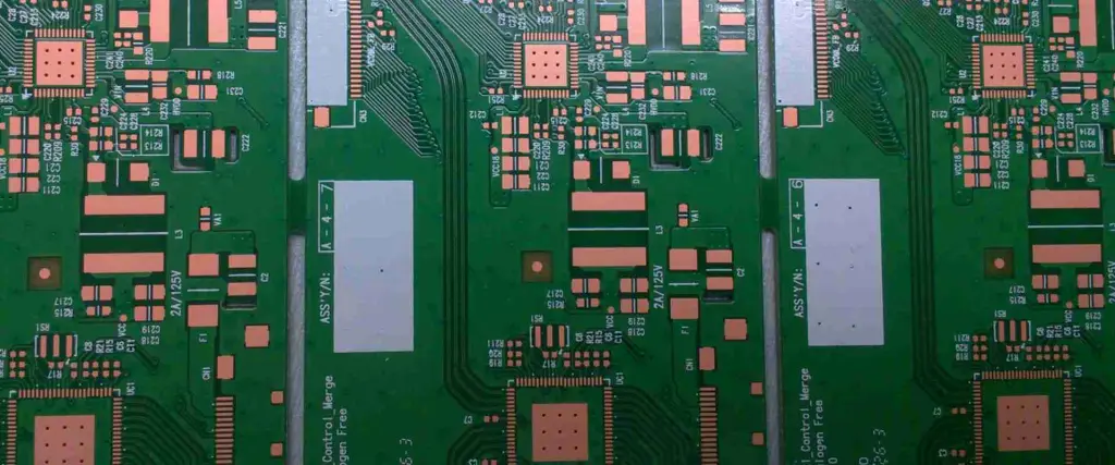
OSP, or Organic Solderability Preservative, is a surface finish applied to the exposed copper pads of a PCB to protect them from oxidation. This thin organic layer, typically made of azole-based compounds, acts as a barrier against environmental factors like moisture and air, which can degrade copper over time. During the soldering process, the OSP coating dissolves, allowing for a clean and reliable connection between the copper and the solder.
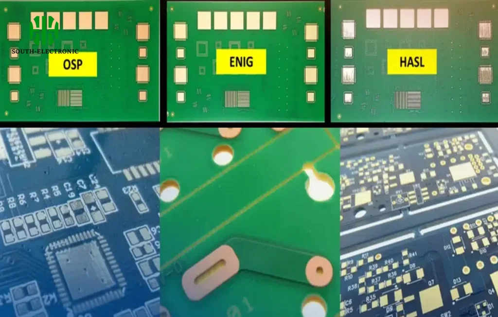
Unlike other surface finishes like HASL (Hot Air Solder Leveling) or ENIG (Electroless Nickel Immersion Gold), OSP doesn't involve heavy metals or complex chemical processes. This makes it a popular choice for manufacturers aiming to meet strict environmental regulations while keeping production costs low. OSP is widely used in consumer electronics, automotive applications, and other industries where lead-free soldering is required.
How Does OSP Finish Work?
The OSP process involves applying a water-based organic compound to the PCB's copper surfaces through a chemical reaction. This reaction forms a protective layer, usually between 0.2 to 0.5 micrometers thick, that bonds with the copper. The layer is thin enough to not interfere with the soldering process but strong enough to prevent oxidation for a limited period.
During assembly, when heat is applied in the soldering process (often at temperatures around 260°C for lead-free solder), the OSP coating breaks down and is removed, exposing the clean copper underneath. This ensures a strong solder joint without residue interference. However, the effectiveness of OSP depends on proper storage and handling, as the coating can degrade if exposed to harsh conditions or excessive touch.
Pros of OSP Finish on PCB
OSP finish offers several advantages that make it a go-to choice for many PCB applications. Below, we break down the key benefits with practical insights to help you understand its value.
1. Cost-Effective Solution
One of the standout advantages of OSP is its low cost. Compared to other surface finishes that require expensive materials or complex processes, OSP uses simple organic compounds and minimal equipment. This can reduce overall production costs by up to 30-40% compared to premium finishes like ENIG, making it an attractive option for high-volume manufacturing where budget is a concern.
2. Environmentally Friendly
OSP is a lead-free and RoHS-compliant surface finish, meaning it aligns with global environmental standards. Unlike some traditional finishes that use harmful substances, OSP relies on organic materials that have a lower environmental impact. For companies prioritizing sustainability, OSP is a step toward greener manufacturing practices.
3. Excellent Solderability
OSP provides a clean copper surface for soldering, ensuring strong and reliable joints. Since the organic layer dissolves during the soldering process, there’s no barrier between the copper and solder, resulting in better wetting and adhesion. This is particularly beneficial in lead-free soldering, where temperatures are higher (often exceeding 250°C), and a clean surface is critical for success.
4. Easy to Rework
If a PCB with OSP finish gets damaged or needs rework, it’s straightforward to strip off the old coating and apply a fresh layer. This reworkability saves time and resources during manufacturing or repairs, as the process doesn’t require specialized tools or extensive labor. For comparison, rework on finishes like ENIG can be more complex due to the multiple metal layers involved.
5. Thin and Flat Surface
The OSP coating is incredibly thin, typically in the range of 0.2 to 0.5 micrometers, which results in a flat surface ideal for fine-pitch components. This flatness ensures uniform contact during soldering, reducing the risk of defects like bridging in high-density PCB designs. For applications with tight tolerances, such as modern smartphones or wearable devices, this is a significant advantage.
Cons of OSP Finish on PCB
While OSP has many benefits, it’s not without its drawbacks. Understanding these limitations will help you determine if OSP is suitable for your specific application.
1. Limited Shelf Life
One of the biggest downsides of OSP is its relatively short shelf life. The organic coating can degrade over time, especially if exposed to high humidity or temperatures above 40°C. Typically, OSP-finished PCBs remain solderable for 6 to 12 months under ideal storage conditions (controlled temperature of 20-25°C and humidity below 60%). Beyond this period, the risk of oxidation increases, potentially leading to soldering failures.
2. Sensitivity to Handling
OSP coatings are delicate and can be easily damaged by fingerprints, dirt, or moisture. Excessive handling during manufacturing or assembly can compromise the protective layer, exposing the copper to oxidation. This sensitivity requires strict handling protocols, such as wearing gloves and using clean environments, which can add to operational complexity.
3. Not Suitable for Multiple Reflow Cycles
OSP is generally not recommended for PCBs that undergo multiple reflow soldering cycles. Each reflow process (often at temperatures of 240-260°C) removes part of the OSP coating, and after two or three cycles, the copper may become exposed and prone to oxidation. For complex assemblies requiring multiple soldering steps, other finishes with higher thermal resistance may be more appropriate.
4. Difficult to Inspect
Unlike metallic finishes that have a distinct visual appearance, OSP is transparent and hard to inspect visually. This makes it challenging to detect whether the coating is intact or has been compromised before soldering. Specialized testing equipment, such as ionic contamination testers, may be needed to ensure quality, adding an extra step to the quality control process.
5. Limited Protection Against Harsh Environments
OSP offers minimal protection against harsh environmental conditions like extreme humidity, corrosive gases, or thermal shocks. For applications in industries such as aerospace or industrial automation, where PCBs are exposed to tough conditions, OSP may not provide the durability needed. In such cases, more robust finishes are often preferred.
When Should You Choose OSP Finish for Your PCB?
Deciding whether OSP is the right surface finish for your PCB depends on several factors, including your project’s budget, environmental requirements, and application needs. Here are some scenarios where OSP shines:
- High-Volume Production:If you’re producing large quantities of PCBs and cost is a primary concern, OSP’s affordability makes it a strong candidate.
- Consumer Electronics:For products like smartphones, tablets, or household appliances with short product cycles and controlled environments, OSP works well due to its solderability and flat surface.
- Lead-Free Compliance:If your project requires adherence to environmental regulations like RoHS, OSP’s eco-friendly nature is a significant plus.
On the other hand, consider alternative finishes if your PCB will face multiple reflow cycles, long storage periods, or harsh conditions. For instance, applications in automotive or outdoor equipment may benefit from more durable options.
How to Maximize the Benefits of OSP Finish
If you decide to use OSP for your PCB, following best practices can help you overcome its limitations and ensure optimal performance. Here are some actionable tips:
- Proper Storage:Store OSP-finished PCBs in a controlled environment with temperatures between 20-25°C and humidity below 60%. Use vacuum-sealed packaging if possible to extend shelf life.
- Minimize Handling:Train staff to handle PCBs with gloves and avoid direct contact with copper pads to prevent contamination of the OSP layer.
- Fast Assembly:Plan your production schedule to assemble OSP-finished PCBs within 6-12 months of manufacturing to avoid degradation.
- Quality Control:Implement testing methods, such as solderability tests per IPC standards (e.g., IPC J-STD-003), to ensure the OSP coating is intact before assembly.
Comparing OSP with Other Surface Finishes
To give you a clearer perspective, let’s briefly compare OSP with two other common surface finishes based on key parameters like cost, shelf life, and solderability. Note that specific values can vary depending on the manufacturer and process.
| Finish Type | Cost (Relative) | Shelf Life | Solderability | Environmental Impact |
|---|---|---|---|---|
| OSP | Low (Approx. $0.10-$0.20 per sq. ft.) | 6-12 months | Excellent (Single Reflow) | Low (Eco-Friendly) |
| HASL (Lead-Free) | Moderate (Approx. $0.30-$0.50 per sq. ft.) | 12-24 months | Good | Moderate |
| ENIG | High (Approx. $1.00-$1.50 per sq. ft.) | 12-24 months | Excellent (Multiple Reflows) | Moderate to High |
This table highlights OSP’s cost advantage and environmental benefits, but also its shorter shelf life and limitations in multiple reflow scenarios. Choose based on your specific project needs.
Conclusion: Is OSP Finish Right for Your PCB?
OSP finish on PCB offers a compelling mix of affordability, eco-friendliness, and excellent solderability, making it a popular choice for many applications. Its thin, flat coating is ideal for fine-pitch components, and its reworkability adds flexibility during manufacturing. However, its limited shelf life, sensitivity to handling, and unsuitability for multiple reflow cycles or harsh environments are important considerations.
By weighing the pros and cons of OSP finish, you can make an informed decision about whether it aligns with your project requirements. If cost and environmental compliance are priorities, and your PCBs will be assembled quickly under controlled conditions, OSP is likely a great fit. For more demanding applications, exploring other finishes might be necessary.
At ALLPCB, we’re committed to helping you select the best surface finish for your PCB designs. With OSP and other options available, we ensure high-quality manufacturing tailored to your needs. Dive into your next project with confidence, knowing you have the right information to make the best choice.
Share · · · ·
The Role of Flux in PCB Wave Soldering: Selection, Application, and Residue Removal
March 16, 2026PCB wave soldering flux types include rosin, water-soluble, and no-clean options with varying activity levels for oxide removal and solder flow. This guide covers selection criteria, spray foam drop-jet application methods, residue removal processes, and alternatives like nitrogen blanketing to boost joint reliability and yields for engineers.
Article
Achieving Uniform Solder Fillets in PCB Wave Soldering: Process Control
March 16, 2026Achieve uniform solder fillets in PCB wave soldering with process control strategies. Optimize flux, preheat, wave height, conveyor speed for consistent fillet shape, height, and wetting balance. Includes visual inspection tips and troubleshooting for reliable through-hole assemblies. Boost quality in production.
Article
Optimizing Conveyor Speed for Efficient PCB Wave Soldering
March 16, 2026Learn PCB wave soldering conveyor speed calculation to manage dwell time, immersion depth, and throughput effectively. Electric engineers get practical steps, best practices, and troubleshooting tips for higher process efficiency and fewer defects in wave soldering operations.
Article
Understanding IPC Standards for PCB Surface Finishes: Ensuring Quality and Compliance
March 11, 2026Understand IPC standards IPC 4552 ENIG and IPC 4553 immersion silver for PCB surface finishes. Ensure compliance, enhance solderability, and prevent common defects to achieve reliable, high quality circuit boards.
Article
Miniaturization Challenges in PCB Assembly
March 11, 2026Navigate the complexities of high density interconnect PCB assembly and precise component placement. Learn to tackle miniaturization challenges, from tiny part handling to thermal stress, ensuring robust and reliable electronics.
Article
High Speed Routing Techniques: PCB
March 11, 2026Master high speed routing in PCBs to ensure signal integrity and minimize electromagnetic interference. Learn essential techniques for robust designs, from controlled impedance to differential pair strategies. Prevent performance issues and achieve reliable electronics.
ArticleGet Instant PCB
Quotations
Full-featured PCB
manufacturing service at low cost.


 相关文章
相关文章


 精彩导读
精彩导读

 热门资讯
热门资讯 关注我们
关注我们